Huawei Kirin 2026 Pro Details and Architecture Emerge
Huawei is accelerating its development of the next-generation Kirin 2026 series, a project that demonstrates the company’s persistent ambition in the semiconductor market despite ongoing international trade restrictions. Recent leaks from reliable industry sources have revealed technical specifications for both the standard and Pro models, highlighting Huawei’s shift toward innovative design strategies. The Kirin 2026 Pro, in particular, utilizes a sophisticated core configuration and a proprietary 3D manufacturing technique known as LogicFolding. These advancements indicate that the company is successfully overcoming hardware limitations to maintain its competitive edge in the global smartphone industry.
- The Kirin 2026 Pro utilizes a nine-core architecture featuring a 3.1 GHz Taishan V4 performance core.
- Huawei implements the proprietary Tau Scaling Law to bypass limitations on advanced lithography equipment.
- The LogicFolding architecture enables a transistor density of 238 million per square millimeter.
- The upcoming processor series will debut in the Huawei Mate 90 smartphone lineup.
The Kirin 2026 Pro Offers Advanced Core Performance
According to reports from the Weibo-based leaker SuperDimensional, the 5G-enabled Kirin 2026 Pro is built upon a 1+4+4 core configuration designed to balance raw power with energy efficiency. The primary super-large core utilizes the new Taishan V4 architecture, capable of reaching peak frequencies of 3.1 GHz. This represents a significant upgrade over the 2.75 GHz speeds seen in the previous Taishan V3-based Kirin 9030 Pro.
The substantial leap in clock speeds marks a new performance milestone for Huawei-designed mobile processors.
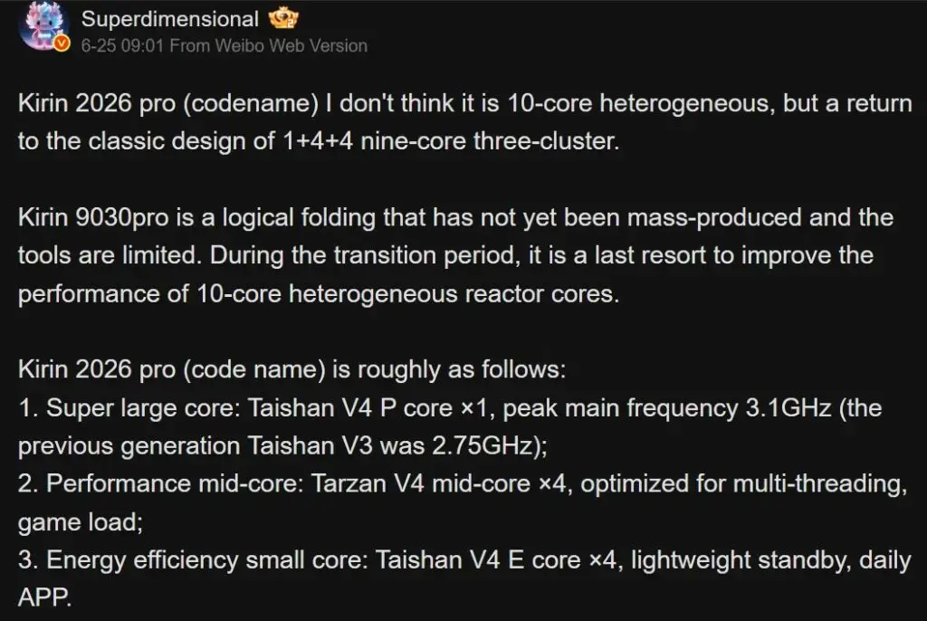
Beyond the primary core, the processor includes four additional Taishan V4 performance cores optimized for multi-threading and gaming applications. The remaining four cores are dedicated to background tasks and efficiency, ensuring that the device maintains responsiveness while conserving battery life. For graphics and artificial intelligence, the chip features an 8-unit GPU and a specialized NPU. The NPU reportedly achieves a dual-layer processing capacity of 100 TOPs and 34 TOPs, providing robust support for modern AI tasks.
The LogicFolding Architecture Redefines Design Standards
Huawei is effectively navigating supply chain challenges by moving away from traditional Moore’s Law, opting instead for its own Tau Scaling Law. By focusing on temporal scaling and signal latency reduction rather than simple geometric shrinking, the company has developed the LogicFolding 3D stacking architecture. This method stacks transistors in layers rather than on a single plane, allowing for a higher concentration of components.
The Kirin 2026 Pro achieves a transistor density of 238 million units per square millimeter, rivaling the world’s most advanced chip manufacturing nodes.
This structural innovation not only facilitates higher component density but also reduces signal path length. Consequently, the processor generates less heat while significantly improving overall response times, marking a major departure from conventional silicon design constraints.
The Huawei Mate 90 Series Will Feature the New Chips
The tech industry anticipates the arrival of the Kirin 2026 series during the launch event for the Huawei Mate 90 smartphone lineup this autumn. While the standard version will likely offer a slightly different feature set, both models are expected to provide high-level efficiency and performance. This launch will serve as a definitive test for Huawei’s new manufacturing philosophy in the consumer market.
What do you think about Huawei’s shift toward the Tau Scaling Law and LogicFolding architecture to overcome hardware limitations; do you believe this design approach will make the Kirin 2026 Pro a top-tier competitor in the mobile market? Share your thoughts in the comments section below.
Your comment has been submitted,
it will be published after approval.