Samsung has taken an exciting step in the tech world by designing its first 3nm mobile processor using AI-powered EDA tools. This chip is the first mobile system-on-chip manufactured using Samsung’s latest 3nm process technology and incorporating gate-all-around transistors (GAAFET). However, the real headline here is that AI was used in the design of this chip.
Samsung’s first 3nm mobile processor was designed with AI
Samsung announced this development alongside Synopsys, demonstrating how AI can streamline the processor design process. Throughout the entire design phase, from architectural planning to physical implementation and verification, these tasks were handed over to machine learning algorithms instead of human engineers.

Synopsys’ AI-based toolkit, Synopsys.ai, includes AI wizards for chip design, functional verification, and silicon testing. These tools analyze data sets using deep learning models and automate typically time-consuming chip development stages.
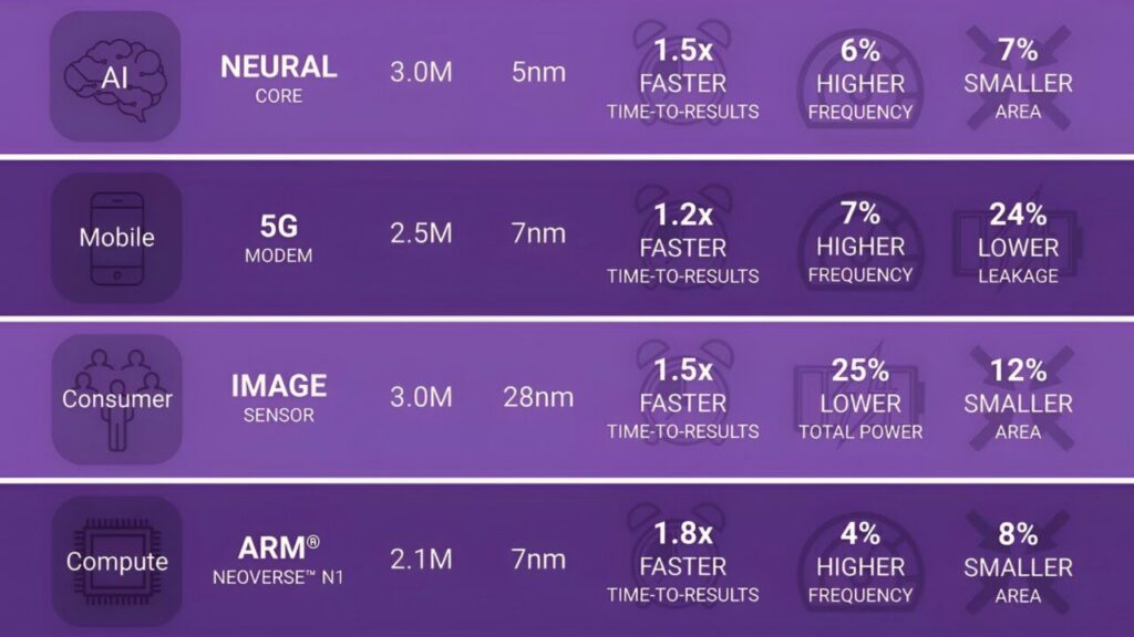
For Samsung’s new mobile processor, AI handled everything from placement to optimization. Thanks to Synopsys’ Fusion Compiler software, Samsung’s team was spared weeks of laborious manual work. With AI-assisted techniques, this 3nm SoC achieved a 300MHz CPU frequency boost and a 10% reduction in dynamic power consumption. These results are impressive for an AI-designed chip.
This design marked Samsung’s first complex design attempt using its latest 3nm GAAFET manufacturing technology. The extensive PPA enhancement capabilities in Synopsys’ AI-focused EDA and IP portfolio enable customers to design chips with the highest quality results for Samsung’s most advanced GAA processes.
Neither Samsung nor Synopsys has detailed exactly which 3nm technology this AI-designed mobile chip uses. However, there is speculation that it employs the second-generation SF3 node. What do you think of this development? Feel free to share your thoughts in the comments section below.


