
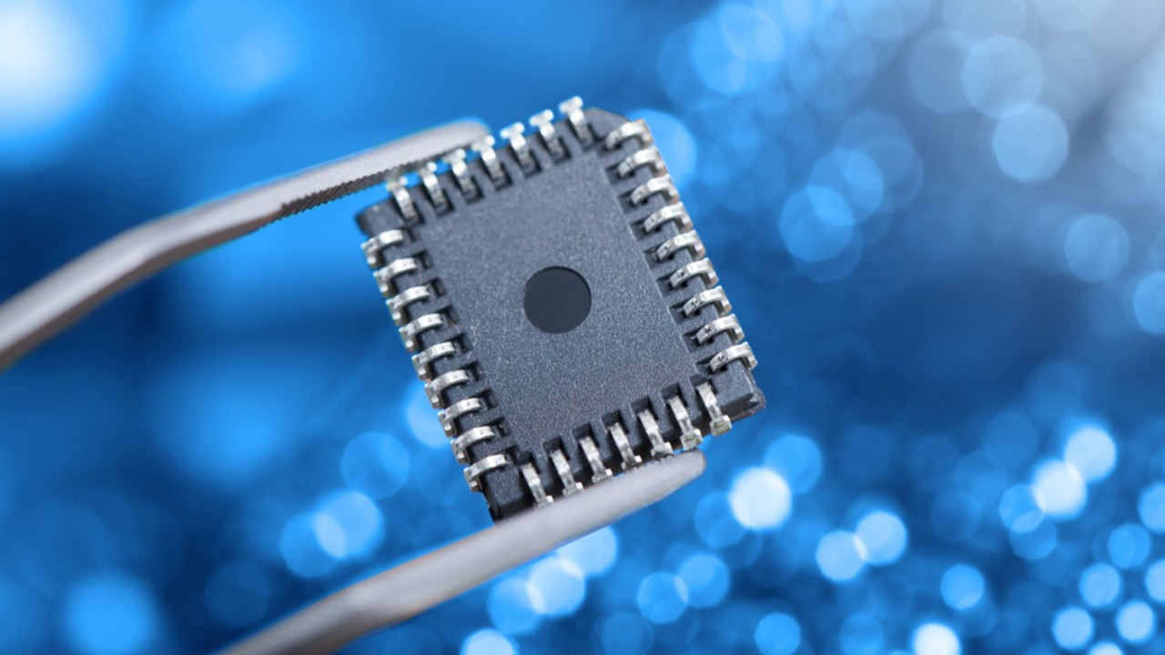
Japan-based semiconductor company Rapidus has reached a significant milestone in its 2-nanometer (nm) manufacturing process. The company has initiated test production of next-generation gate-all-around (GAA) architecture transistors at its IIM-1 facility in Chitose. This step is considered one of the most critical technical milestones before mass production, scheduled for 2027.
Rapidus to Begin 2nm Chip Production
The 2nm chips produced in test production met the expected electrical performance parameters. Basic technical measurements, such as threshold voltage, conduction current, leakage current, and transition slope, were taken on the produced samples.
Rapidus has not publicly released these measurement results, but the fact that test chips are moving through the production line indicates that production tools are operating at target performance and that the R&D process is technically progressing successfully.
Infrastructure preparations for test production at Rapidus’ IIM-1 facility began in September 2023. The clean room was completed in 2024. As of June 2025, over 200 production tools, including DUV and EUV lithography tools, were commissioned.
Advanced EUV systems were installed in December 2024 and used in initial production trials by April 2025. Thanks to this infrastructure, Rapidus began producing test plates and demonstrating its 2nm production capabilities in practice.
The company’s production approach is also noteworthy. Rapidus announced that it will implement single-wafer processing in all production steps. In this system, each wafer is processed and inspected individually.
While manufacturers such as TSMC, Samsung, and Intel currently use this method only in select steps, Rapidus plans to implement the entire process in this manner, including processes such as oxidation, ion implantation, and cleaning. This method allows for real-time analysis of each wafer. Errors can be detected early, parameters can be optimized, and production efficiency can be increased.
However, this system also presents some technical and economic challenges. Processing wafers individually increases production time and costs. Additionally, the required equipment is more complex and expensive. Despite this, Rapidus anticipates that this method will provide a competitive advantage in the long term for 2nm and higher-end technologies thanks to its lower error rate, higher efficiency, and flexible manufacturing infrastructure.
The company also plans to release its first process development kit (PDK) to customers in the first quarter of 2026. This kit will enable design on Rapidus’s 2nm technology.