iPhone Air’s motherboard revealed! Interesting detail
Apple has unveiled its new iPhone Air, which stands out with its ultra-thin body. Images shown during the launch suggested the company had tucked all components within the camera bump to maintain its slimness. However, the latest motherboard design diagrams suggest otherwise.
iPhone Air motherboard examined
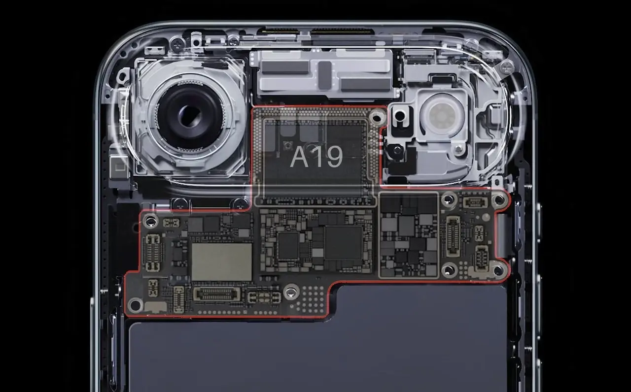
Leaks indicate that the A19 Pro chip occupies a significant portion of the motherboard. The motherboard itself is designed in a “sandwich” structure, with components positioned on either side to save space. Key components such as the C1X 5G modem and the N1 wireless communication chip are also positioned on either side of this motherboard. The company appears to have managed to save space by using its own chips.
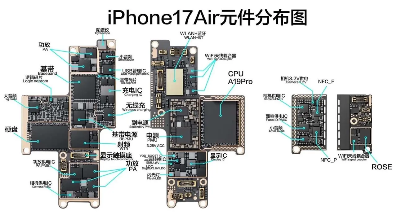
However, despite all these efforts, Apple hasn’t been able to shrink the main circuit board enough to fit entirely within the camera bump. Renderings shared on social media clearly reveal the motherboard’s positioning inside the phone, and the image shows only the A19 Pro chip nestled within the camera bump. The impression that the entire motherboard has been moved there is incorrect.
Over the next few generations, Apple is expected to further shrink motherboard designs, fitting all components into the camera cluster and allocating the remaining space to a larger battery, which is considered a potential future development. However, the first teardown videos are expected to be released to confirm whether the motherboard is truly this way.
So, what are your thoughts on this? Share your thoughts with us in the comments section below.
Your comment has been submitted,
it will be published after approval.