TSMC to Launch Revolutionary CoPoS Technology by 2028
Semiconductor manufacturing giant TSMC is set to revolutionize the artificial intelligence hardware industry by launching its next-generation CoPoS (chip-on-panel-on-substrate) packaging technology in the second half of 2028. According to industry analyst Ming-Chi Kuo, this advanced manufacturing solution aims to overcome the physical limitations of current CoWoS packaging, enabling the production of significantly larger chip designs. NVIDIA is expected to be among the primary adopters of this technology for its upcoming Feynman artificial intelligence chips. By shifting toward a glass-core structure, TSMC intends to meet the surging global demand for enhanced processing power while maintaining its leadership in the semiconductor market.
- TSMC will transition to mass production of its CoPoS technology in the latter half of 2028.
- The new packaging architecture enables the production of chip surfaces nine times larger than standard lithography templates.
- NVIDIA will integrate this advanced packaging solution into its future Feynman-coded AI processors.
- The CoPoS method utilizes a glass-core design with ABF layers to replace traditional silicon interposers.
CoPoS Technology Redefines Physical Manufacturing Limits
The current industry-standard CoWoS (chip-on-wafer-on-substrate) technology has reached a technical bottleneck due to the inherent size constraints of silicon interposers. These physical limits hinder the development of ultra-large-scale artificial intelligence chips required for modern data centers. TSMC’s CoPoS technology bypasses these constraints by utilizing a panel-level approach that removes the need for traditional interposers entirely. By mounting components directly onto the panel, manufacturers can finally scale beyond existing lithography machine limitations.
TSMC’s innovative methodology enables the production of massive chip designs exceeding 9.5 times the current reticle size.
Glass-Core Designs Improve Thermal Performance
A critical component of this transition involves the integration of a glass core sandwiched between Ajinomoto Buildup Film (ABF) layers. As noted by analyst Ming-Chi Kuo, this structure provides a significantly more stable foundation for high-performance computing components. 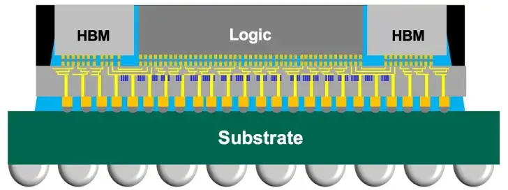 This architecture does not only improve the structural integrity of the chips but also optimizes thermal management and signal transmission speeds. Compared to existing packaging methods, the CoPoS process offers greater manufacturing flexibility, which is essential for companies like NVIDIA that require high-performance hardware to drive complex AI workloads.
Strategic Partnerships Secure Future Market Dominance
While rumors have suggested that NVIDIA might explore Intel’s EMIB-T packaging solutions, TSMC’s aggressive roadmap for CoPoS signals a strategic move to solidify its long-standing partnership with the AI chip designer. As the industry approaches 2028, the shift in chip architecture represents a fundamental change in both technical capabilities and cost efficiency. Analysts suggest that if TSMC successfully implements this technology at scale, the firm will effectively maintain its stronghold in the high-end packaging market, distancing itself from competitors attempting to catch up with similar innovations.
As the semiconductor industry prepares to shift toward glass-core packaging by 2028, what significant impacts do you foresee for the future of artificial intelligence hardware performance? Share your thoughts and predictions in the comments section below.
Your comment has been submitted,
it will be published after approval.