Despite major sanctions from the US, Huawei continues to advance at full speed in semiconductor technologies. The company continues its preparations to start trial production in the 3nm production process in 2026.
Huawei moves to 3nm chip production
GAA (Gate-All-Around) transistor technology and two-dimensional materials will be used in the new generation chips to be developed. This production process is based on a new architecture that offers higher performance and energy efficiency.
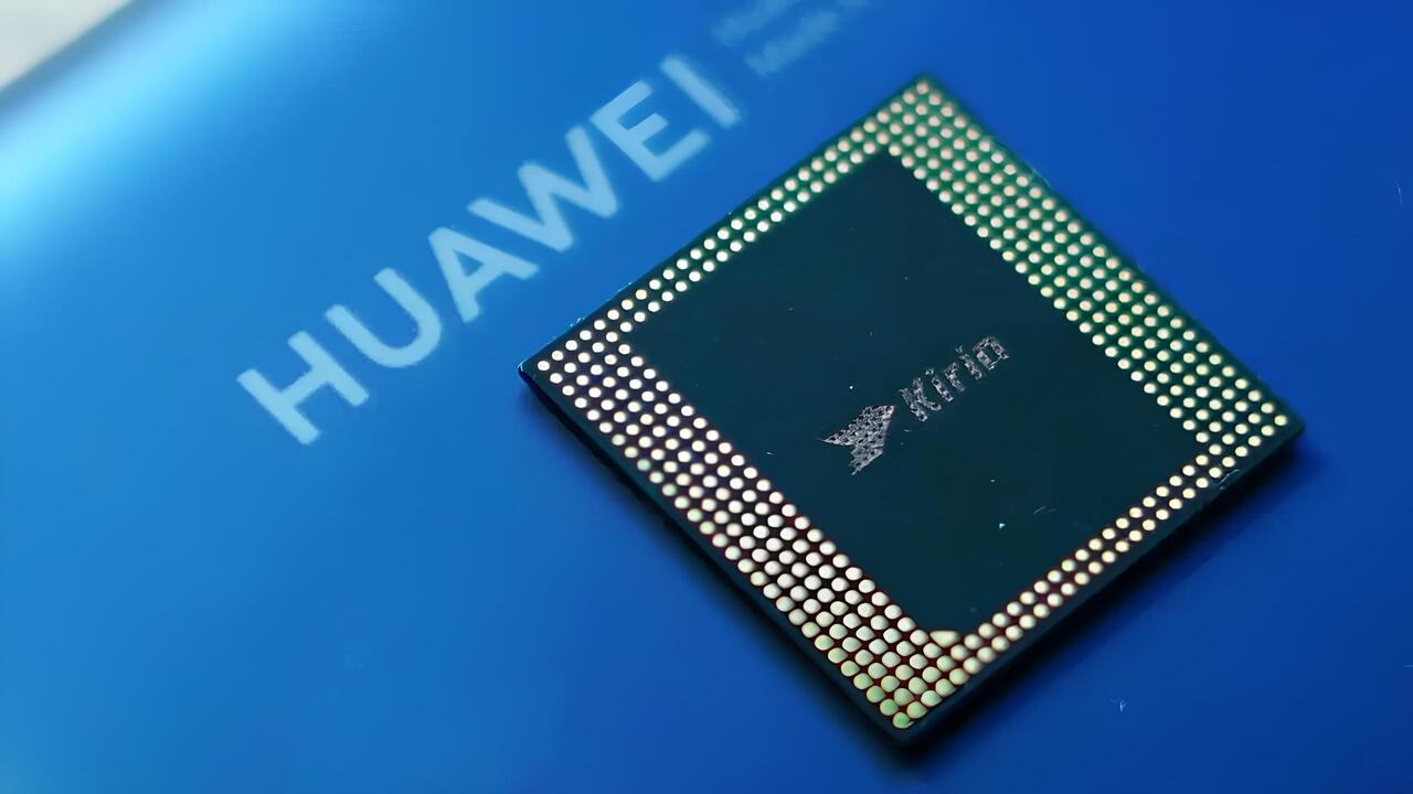
All suppliers using US technologies are prohibited from selling to Huawei. Huawei, which used its chip stocks during this process, later returned to the market with the Kirin 9000S chip developed with SMIC’s 7nm production process.
The first computer with the HarmonyOS operating system announced at the beginning of May used the Kirin X90 chip, which was stated to be developed with the 5nm process. In the analyses, it is stated that SMIC’s 7nm production process, called N+2, and JCET’s 4nm level packaging technology were used in the production of this chip.
SMIC’s most advanced production process, 7nm, is reported to have an efficiency rate of 50%. The main reason for this low efficiency was China’s lack of access to EUV (Extreme Ultraviolet) lithography machines.
Huawei is working with Chinese equipment manufacturers to eliminate its dependence on EUV lithography in 5nm technology. SSA800 series stepper systems developed by Shanghai Micro Electronics are used in lithography machines.
In studies conducted within the company, it is stated that 3nm level carbon nanotube-based chips have also passed laboratory verification. The process of adapting these carbon-based chips to the production line at SMIC facilities is ongoing.
So what do you think about this issue? You can share your views with us in the comments section below.