
Intel Challenges TSMC with Advanced EMIB-T Packaging Technology by 2027

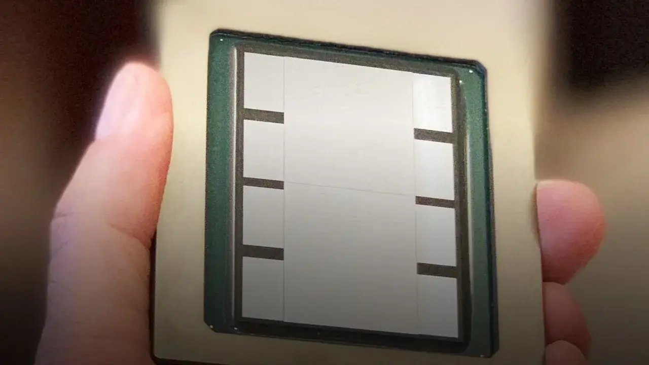
Intel is aggressively expanding its foundry capabilities to compete with industry leader TSMC, announcing that its advanced EMIB-T packaging technology is scheduled for high-volume production by 2027. By leveraging its proprietary Embedded Multi-die Interconnect Bridge (EMIB) architecture, Intel aims to offer ASIC designers a more cost-efficient and high-performance alternative to traditional silicon interposer solutions. As the semiconductor landscape faces increasing demands for massive bandwidth and power density, Intel is positioning its suite of packaging variants, including EMIB, EMIB-M, and EMIB-T, to attract major global clients currently relying on TSMC’s CoWoS ecosystem.
- Intel plans to initiate high-volume production of its EMIB-T packaging technology by 2027.
- EMIB-T architecture provides a cost reduction of up to 50 percent compared to traditional CoWoS methods.
- Designers are exploring Intel’s technology as a viable alternative due to technical challenges reported in competing packaging designs.
EMIB-T Technology Offers Significant Cost Advantages
The core innovation behind Intel’s strategy is the EMIB-T variant, which utilizes Through-Silicon Via (TSV) technology to provide direct access to power connections. This design capability allows for multi-kilowatt solutions within a single package, maintaining high bandwidth without the prohibitive costs associated with full-size silicon interposers. According to projections from production partner Unimicron, this technology will be ready for widespread commercial adoption in less than three years.
The significant price disparity between Intel’s EMIB-T and competing interposer-based packaging allows clients to reallocate budgets toward other critical areas of chip development.
Major ASIC designers, including industry giants like Meta and Broadcom, are reportedly evaluating a transition to Intel’s packaging ecosystem. By bypassing the need for expensive, large-scale silicon interposers, companies can maintain the necessary performance density while optimizing their overall system-level expenditures. This pivot marks a strategic effort by Intel to capture market share from TSMC by addressing the specific economic and technical constraints faced by modern chip architects.
TSMC Faces Technical Hurdles in Advanced Packaging
While TSMC has long dominated the advanced packaging sector, recent reports suggest the company is encountering friction with its CoWoS-L designs, particularly regarding the Vera Rubin architecture utilized by NVIDIA. Allegations of package warping have led to concerns about physical contact failures between processor dies and the underlying substrate. These challenges have prompted some industry players to look toward Intel’s proven EMIB methodology as a more reliable and cost-effective alternative for multi-die configurations.
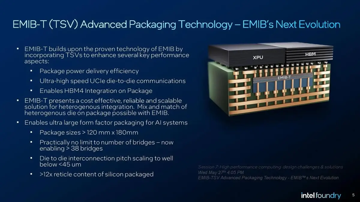
Intel’s strategy involves scaling its EMIB offerings to support diverse needs, ranging from high-bandwidth memory integration to complex multi-die systems. By offering a more modular and potentially more stable packaging environment, the company hopes to stabilize its foundry growth and provide a compelling alternative for next-generation AI and data center hardware.
What are your thoughts on this competitive shift in the semiconductor industry, and do you believe Intel can effectively disrupt TSMC’s market dominance with its new packaging technologies? Share your insights in the comments section below.
Your comment has been submitted,
it will be published after approval.