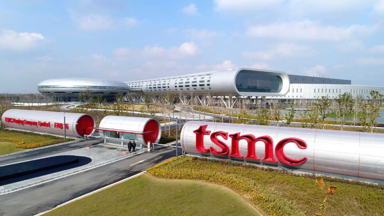
Taiwan Semiconductor Manufacturing Company (TSMC) has officially begun construction on its new 1.4nm (A14) fabrication facility, which it claims will be the world’s most advanced semiconductor manufacturing facility. The cost of this massive project, located in Taiwan’s Central Taiwan Science Park, has been announced as $48.5 billion. According to UDN, TSMC quietly began groundbreaking work on its next-generation manufacturing facility recently.
TSMC is building its most comprehensive chip facility
This facility, designated “Fab 25,” will feature a total of four separate 1.4nm wafer production lines. According to plans, risk production on the first line is expected to be completed by the end of 2027. Mass production is expected to begin in the second half of 2028. The company aims to reach a monthly production capacity of approximately 50,000 wafers with this facility.
The new 1.4nm A14 fabrication process offers significant gains in energy efficiency and density compared to the current 2nm technology. This cutting-edge production line will be used not only by mobile-focused customers like Apple, Qualcomm, and MediaTek, but also by high-performance artificial intelligence (AI) chip manufacturers like NVIDIA and AMD.
TSMC has recently accelerated its investments amid rising costs and global demand. With new facilities in Taiwan, the US, and Japan, the company is both diversifying its production line and increasing capacity. The transition to the 1.4nm process is positioned as the most critical step in this global growth strategy.