Samsung Electronics is preparing for a radical change in chip packaging technology. It was stated that the company will switch from traditional silicon-based interlayers to glass-based interlayers by 2028. This transformation will be critical, especially in terms of increasing the performance of artificial intelligence chips and reducing production costs.
Samsung may use glass instead of silicon in its chips
Interlayers used in chip production play an important role especially in 2.5D packaging technology, where high-bandwidth memories (HBM) are combined with GPUs. Until now, silicon was mainly used in this area.
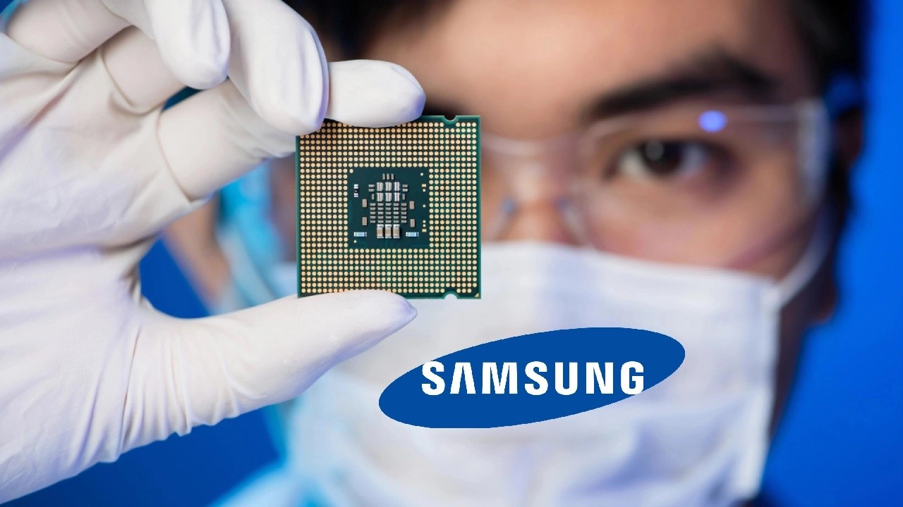
However, silicon interposers have disadvantages such as high production costs and limited production flexibility. It is stated that Samsung is also turning to glass-based solutions for this reason. Glass; It stands out with its stability and low production costs, while offering more precision for ultra-thin circuit structures.
These features provide significant advantages in the production of new generation chips developed for large data centers and applications requiring intensive artificial intelligence processing power. Glass substrates both allow for higher-density circuit design and are much more resistant to thermal expansion.
While the interest in glass interlayers is increasing in the industry, Samsung seems to be charting its own path in this area. Many manufacturers continue to work on large-sized glass panels (510×515 mm). However, Samsung is focused on more compact glass units under 100×100 mm.
So what do you think about this? You can share your views with us in the comments section below.