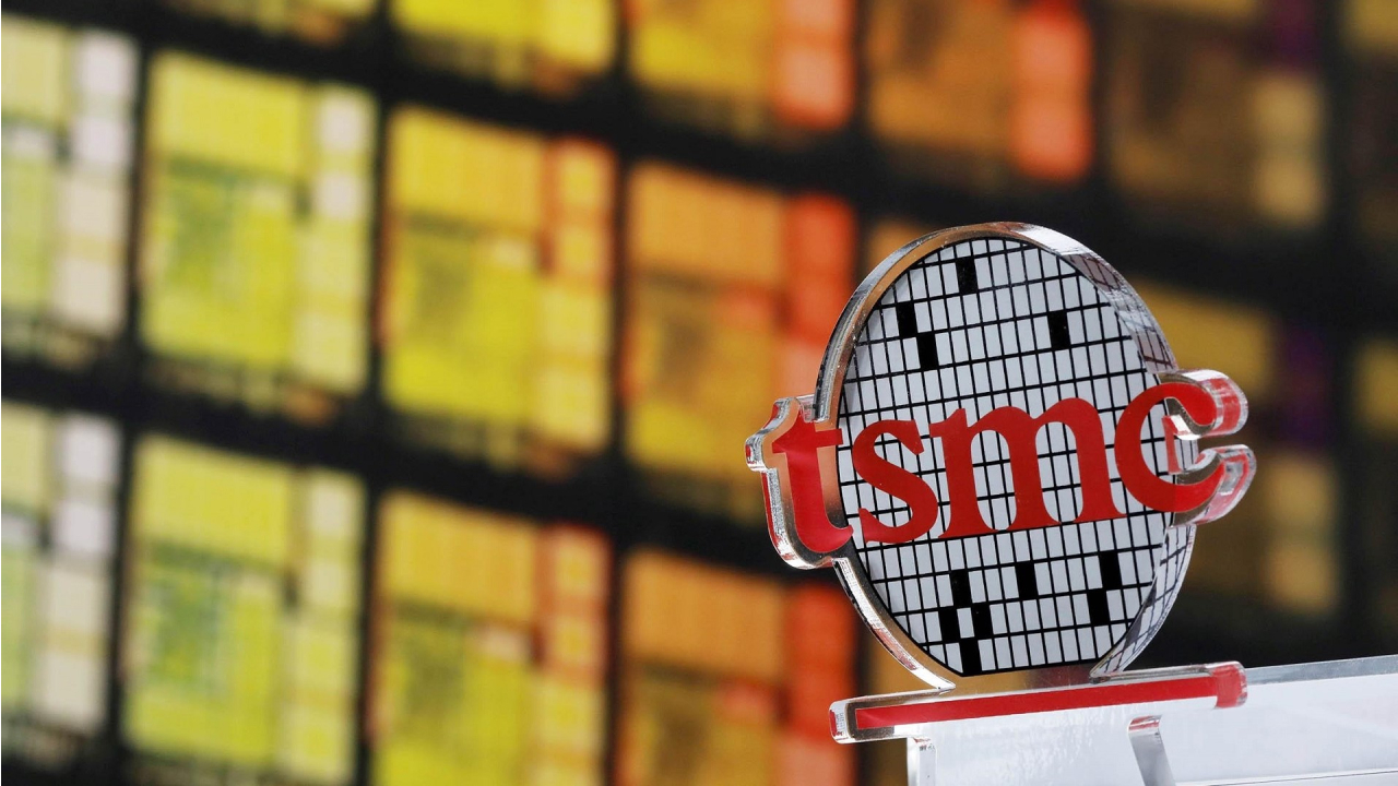
Semiconductor manufacturer TSMC announced a significant leap forward in chip design with its new 1.4-nanometer-class A14 process. The company clearly demonstrated that this advanced technology will deliver significant gains in performance and power efficiency.
TSMC Will Offer Significant Performance Increases
TSMC reports that it has achieved higher-than-expected efficiency from trial production, confirming that development is ahead of schedule. The A14 process is slated to enter mass production in 2028.
According to information shared by analyst Ray Wang, the A14 semiconductor process offers significant improvements over TSMC’s current 2-nanometer (N2) platform. The new technology delivers up to a 15 percent performance increase when measured at the same power level.
When operating at similar speeds, power consumption is reduced by up to 30 percent. Furthermore, in terms of density, A14 allows for the integration of up to 20 percent more transistors than N2.
TSMC stated that these significant advancements were achieved thanks to innovations such as the second-generation GAA nanosheet transistor architecture and the NanoFlex Pro design standard. The company’s advancement of development plans reinforces its goal of putting the A14 process into production by 2028.
TSMC’s release of detailed technical data on the A14 demonstrates that the company is ahead of its competitors, Samsung and Intel. While these companies have announced their roadmaps for future transistor architectures, they have not provided as much concrete and detailed data on performance and efficiency improvements as TSMC.
With this breakthrough, TSMC has proven its readiness for post-2-nanometer technologies. The new manufacturing process has become a vital development in the industry, directly impacting the performance and energy efficiency of next-generation products for major customers such as Apple, Nvidia, and AMD.