
Micron Unveils Revolutionary 400-Layer G11 3D NAND SSD Technology

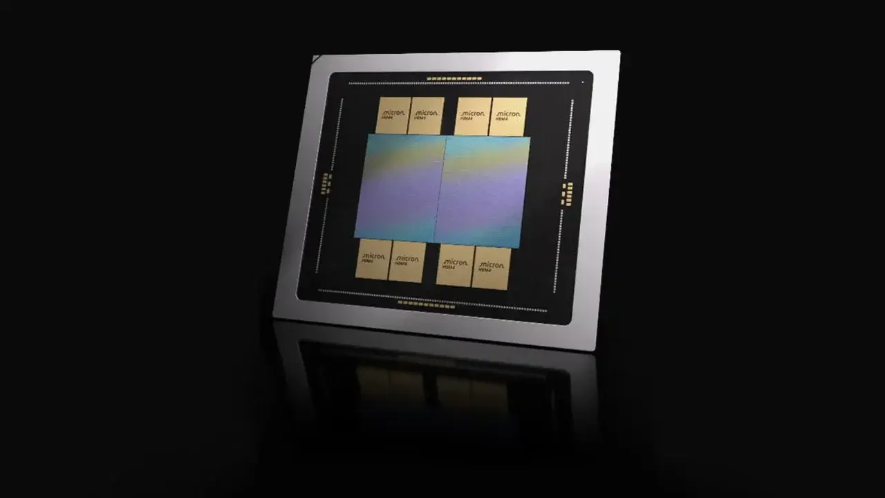
Memory manufacturer Micron has officially announced its next-generation Micron G11 3D NAND technology, which features an architecture boasting over 400 layers. This massive leap in storage engineering doubles the data density compared to the company’s current G9 generation, representing a significant milestone for the industry. Unveiled as a major advancement, the technology promises a 50 percent increase in input/output performance while simultaneously reducing energy consumption during data transfers. Micron plans to commence mass production of these high-capacity memory chips in the second half of 2027, setting the stage for future high-performance computing and enterprise-grade storage solutions.
- Micron will implement a wafer-on-wafer bonding process to integrate the memory array with control and I/O circuits.
- The G11 architecture aims to reach a storage density of approximately 42 Gbit/mm² by effectively doubling current capacity.
- Data transfer speeds are expected to climb to 5,400 MT/s, which represents a 1.5x performance boost over the previous generation.
- Energy efficiency will improve significantly as the new design targets a reduction of over 25 percent in power consumption per bit.
Micron Bypasses G10 to Advance Storage Density
In a strategic move to accelerate innovation, Micron has decided to skip the G10 generation entirely, moving directly from G9 to the G11 3D NAND architecture. The primary focus of this development is to maximize the density of memory cells within a smaller physical footprint. By utilizing advanced wafer-on-wafer bonding, Micron can manufacture memory arrays and logic circuits separately before joining them, which optimizes both yield and performance.
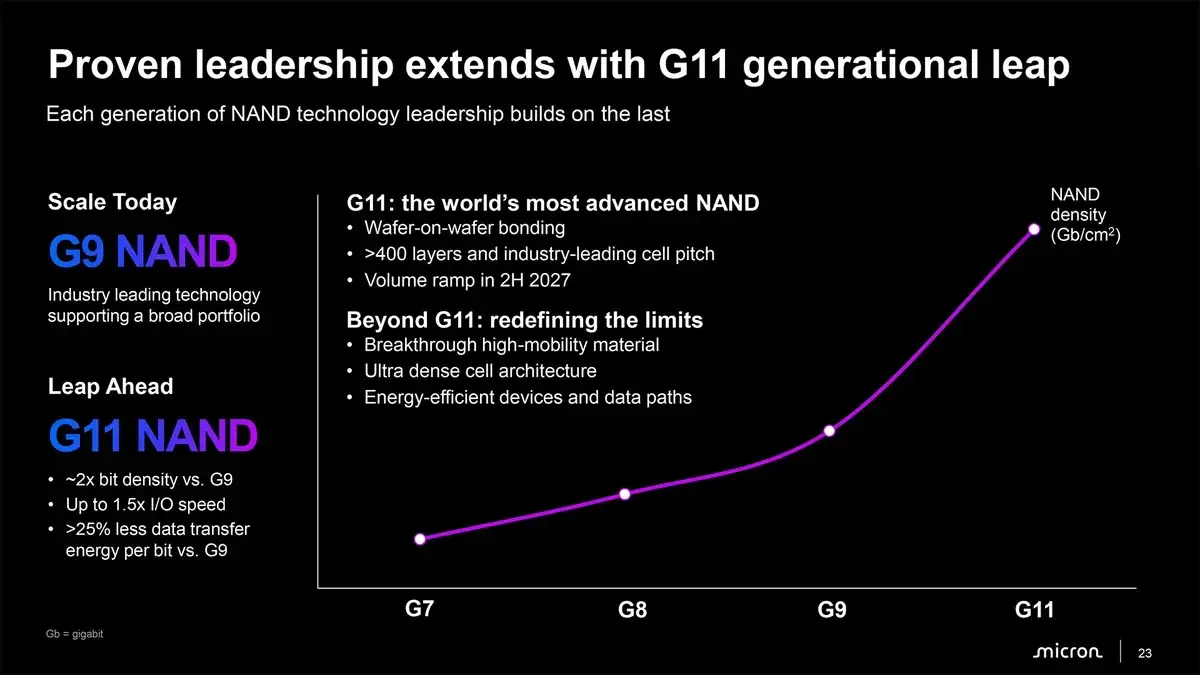
The technical specifications are equally impressive, as the new architecture aims to achieve a density of 42 Gbit/mm², compared to the 21 Gbit/mm² found in the current G9 generation. This doubling of bit density allows manufacturers to provide significantly more storage capacity within the same physical silicon area, ultimately driving down costs for high-capacity drives.
Performance Standards are Being Raised Significantly
The performance metrics of the G11 technology are designed to meet the growing demands of modern data centers and artificial intelligence workloads. With an interface speed theoretically capable of reaching 5,400 MT/s, the G11 architecture is engineered to handle massive data throughput with ease. 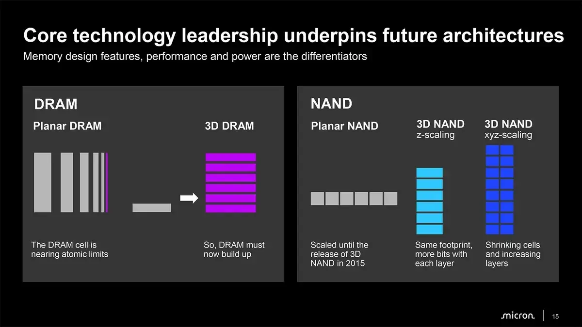 Furthermore, the reduction in power consumption by more than 25 percent per bit is a critical improvement for large-scale server environments where energy costs and heat management are major concerns.
Market Competition is Intensifying Rapidly
As Micron prepares for the 2027 production cycle, it faces stiff competition from industry rivals such as Samsung and Kioxia, who are also developing next-generation NAND solutions like V10 and BiCS10. Micron’s strategy involves not only increasing the number of vertical layers but also reducing the physical distance between cells to maintain a competitive edge. Looking beyond the G11 release, the company continues to research new semiconductor materials that offer higher carrier mobility, ensuring that future iterations will continue to push the boundaries of 3D scaling.
As storage capacities continue to scale into the hundreds of layers, we are curious to hear your thoughts on how this massive increase in available data will impact your daily digital life; please share your comments below regarding whether you believe these advancements will change how we manage our personal files.
Your comment has been submitted,
it will be published after approval.