
Huawei Pioneers 3D Stacking Technology for 7 Nanometer Processors

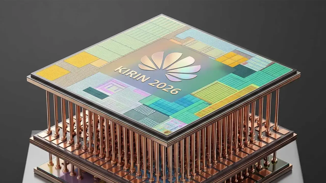
Huawei is making a significant technological shift by integrating 3D stacking and hybrid bonding into its next-generation Kirin processors, aiming to maintain its competitive edge in the global smartphone market. Despite facing restricted access to advanced lithography equipment, the company is leveraging these innovative packaging techniques to enhance data processing speeds and optimize energy efficiency at the 7 nanometer node. By moving away from traditional planar designs, Huawei intends to maximize the performance of its existing hardware architecture. This strategic pivot highlights the company’s commitment to overcoming manufacturing limitations through advanced engineering and creative semiconductor design solutions in a highly competitive industry landscape.
- Huawei adopts 3D chip stacking and hybrid bonding to mitigate performance bottlenecks.
- This architectural shift reduces latency by minimizing the physical distance between internal components.
- The company achieves improved efficiency without requiring access to extreme ultraviolet lithography tools.
- Industry leaders including Apple and Samsung are simultaneously pursuing multi-chip packaging technologies.
Three-dimensional packaging technology represents the most significant transformation in Huawei’s hardware architecture to date.
Components are Being Placed in Vertical Stacks
The new methodology adopted by Huawei involves stacking core components, including the processor, graphical processing units, AI cores, and memory modules, on a vertical plane. Unlike conventional flat layouts where data must travel across longer horizontal paths, the 3D stacking approach utilizes thousands of high-density vertical interconnects. This dense integration allows for faster communication between modules while maintaining strict control over overall power consumption.
As modern smartphones become increasingly reliant on on-device artificial intelligence, managing the data flow between memory and the processor is essential. By eliminating the traditional data bottleneck, this vertical structure ensures that high-demand tasks are handled with greater efficiency, directly improving the user experience and device responsiveness.
Sanctions are Being Overcome Through Architectural Design
Due to ongoing international trade restrictions, Huawei remains unable to utilize the latest extreme ultraviolet (EUV) lithography machines, forcing a reliance on SMIC’s 7 nanometer production processes. Rather than accepting these hardware limitations, the company is compensating by advancing its chip packaging expertise. This approach demonstrates that engineering brilliance can often serve as a viable alternative to raw lithographic node progression.
Advanced packaging methods are effectively pushing the physical boundaries of the 7 nanometer process.
Industry analysts emphasize that this shift toward advanced packaging is becoming an global industry trend rather than a solitary Huawei strategy. Reports suggest that Samsung is preparing to separate memory and computation units in its Exynos 2700 chipset, while Apple is reportedly integrating WMCM multi-chip packaging for its upcoming A20 Pro processors. The semiconductor industry is clearly moving toward a future where internal layout and heterogeneous integration are just as vital as shrinking the size of individual transistors.
The Future of Competition is Being Reshaped
Huawei’s bold move into 3D stacking could signify the beginning of a new era for smartphone processors. Even with manufacturing constraints, the company is proving that sophisticated design choices can yield massive performance gains. As these multi-layer chip architectures become the industry standard in the coming years, the focus will continue to shift toward how effectively manufacturers can integrate complex systems within a confined space.
Do you believe that Huawei’s 3D stacking strategy will be enough to close the performance gap with its major competitors? We invite you to share your thoughts and technical predictions in the comments section below.
Your comment has been submitted,
it will be published after approval.