The graphic monster is coming! AMD Strix Halo Zen 5 APU

Exciting details have emerged about AMD’s brand-new AMD Strix Halo Zen 5 APU. This graphics powerhouse, equipped with RDNA 3.5 technology, features a massive 307 mm² graphics chip. What can this new chip offer us? Here are the details…
AMD Strix Halo Zen 5 APU Graphics Chip Features
The AMD Strix Halo Zen 5 APU comes with FP11 packaging, which has a size of 37.5×45 mm, equivalent to Intel’s LGA-1700 socket panel. This means AMD’s new APU is set to compete head-to-head with Intel’s high-end processors. The largest graphics chip contains the RDNA 3.5 graphics module and measures 307 mm².
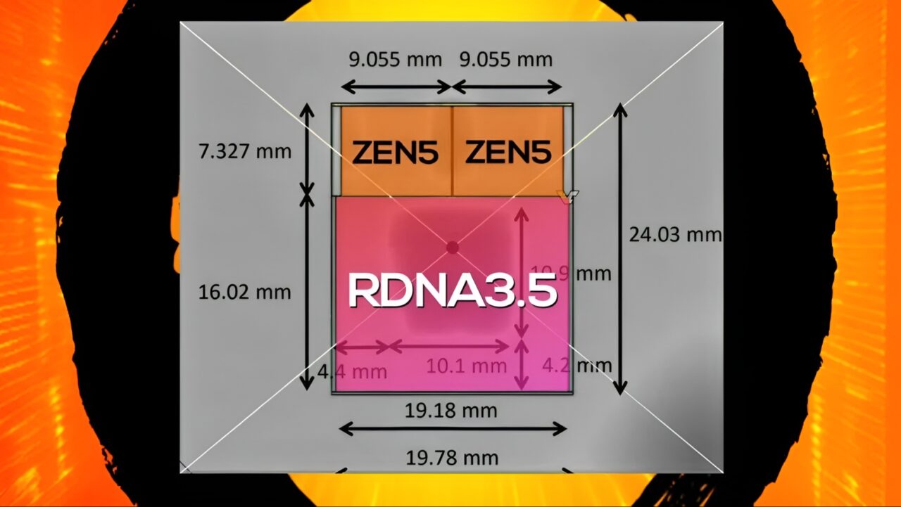
Additionally, it includes two CCD chips, each providing 8 Zen 5 cores, with each CCD measuring 66.3 mm².
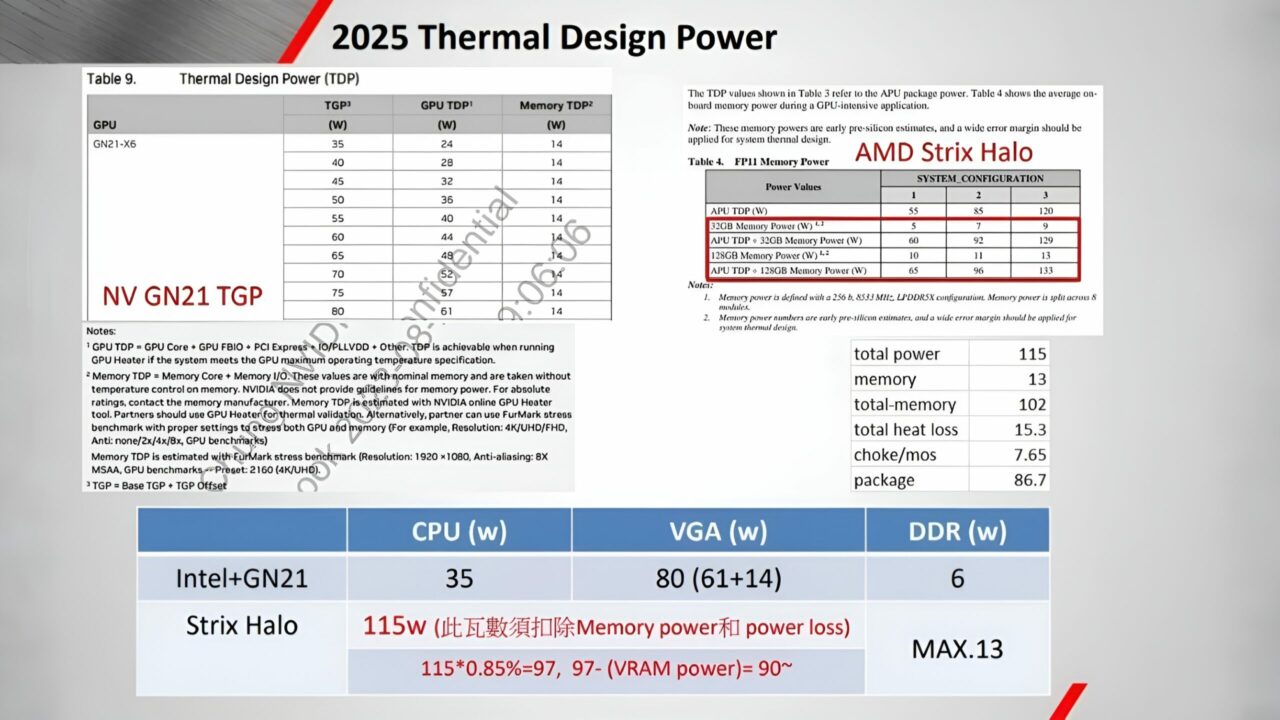
The “Strix Halo” Zen 5 APU has thermal design power (TDP) ratings of 55W, 85W, and 120W, excluding memory power. AMD estimates the memory power consumption as 9W for a 32GB system and 13W for a 128GB system. This means the new APU promises high performance while also focusing on energy efficiency.
What is AMD Amuse 2.0 AI and how to use it?
The RDNA 3.5 graphics technology is expected to deliver superior performance in gaming and graphics processing. This means smoother games, more vibrant graphics, and faster workflows.
What do you think about this new APU? Share your thoughts in the comments below.
Your comment has been submitted,
it will be published after approval.