
TSMC Gears Up for Massive 2nm Chip Production

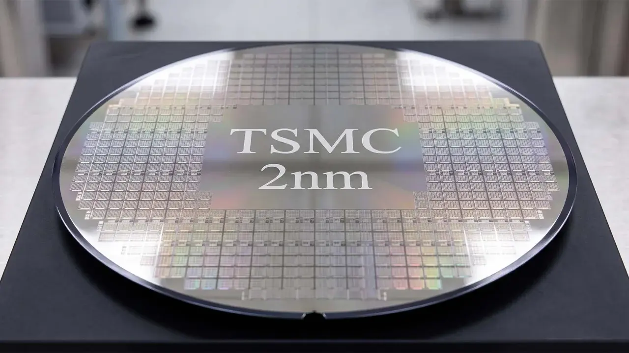
TSMC, the world’s leading semiconductor foundry, has reached a critical milestone in transitioning from 3nm to 2nm chip production technology. As of the current development phase, the company’s manufacturing facilities have achieved a monthly output capacity of 20,000 wafers specifically dedicated to the next-generation 2nm process. With five specialized facilities in Taiwan focusing exclusively on this technology, TSMC is accelerating its infrastructure expansion, particularly at its Fab 20 site, to accommodate surging global demand. This strategic shift marks a pivotal moment for the semiconductor industry as manufacturers prepare to integrate these highly advanced components into upcoming consumer electronics and artificial intelligence systems.
- TSMC has successfully ramped up its 2nm production capacity to 20,000 wafers per month.
- Apple and Google are expected to debut the first 2nm-based system-on-chip designs starting in late 2026.
- The artificial intelligence sector acts as the primary driver for the rapid adoption of 2nm process nodes.
Apple and Google Lead the 2nm Transition
The semiconductor landscape is bracing for a significant technological leap as major tech giants prepare for the implementation of 2nm chips. Although these components have not yet reached mass market circulation, industry data shows that 2nm design approvals have surged to four times the volume observed during the 3nm transition period. This level of adoption signals strong confidence from major designers regarding the efficiency gains promised by the new lithography process.
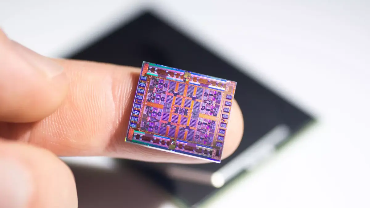
Industry analysts anticipate the launch of the Google Pixel 11 series, featuring the Tensor G6, and the iPhone 18 series, powered by the A20 Pro chip, to signify the official arrival of 2nm consumer hardware.
While the 3nm node currently remains the backbone of TSMC’s output with 175,000 wafers per month, the transition to 2nm is inevitable. As AI-focused companies migrate their designs to the newer process, 2nm technology is projected to become the primary revenue stream for the foundry in the coming years.
Artificial Intelligence Demand Shapes Production Strategies
The artificial intelligence sector is currently the dominant force influencing TSMC’s manufacturing roadmap. AMD has formally announced that its MI455X GPU, designed specifically for agentic AI workloads, will utilize the 2nm process node. Furthermore, industry experts expect NVIDIA’s upcoming Rubin architecture to enter the 2nm ecosystem, further intensifying the competition for advanced manufacturing capacity.
TSMC aims to cement its long-term technological leadership by focusing the majority of its 2nm production volume on high-performance artificial intelligence chips.
The shift toward 2nm is not merely a quantitative increase in production but a qualitative leap in computational efficiency and power management. As the industry moves toward more complex neural networks, the demand for smaller, more efficient transistors becomes an operational necessity for major chip designers worldwide. By positioning itself at the forefront of this manufacturing evolution, TSMC continues to dictate the pace at which the global tech industry evolves.
Given the rapid advancements in semiconductor manufacturing, we invite you to share your perspective on whether 2nm technology will deliver the performance breakthroughs required for the next generation of artificial intelligence and mobile devices.
Your comment has been submitted,
it will be published after approval.