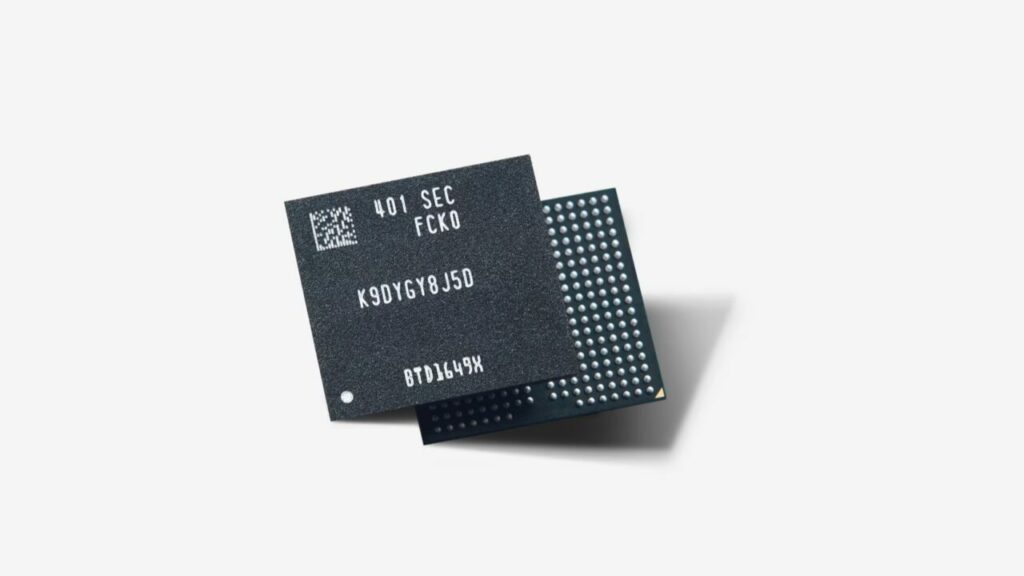
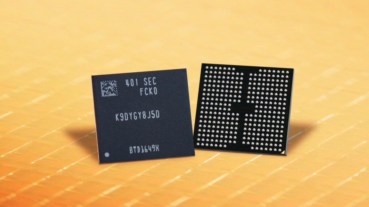
Samsung Electronics, a leader in advanced memory technology, announced the start of mass production for its 9th-generation vertical NAND (V-NAND). This new generation of V-NAND features a triple-level cell (TLC) structure with a 1 terabit (Tb) capacity, reinforcing its leadership in the NAND flash market.
Samsung begins mass production of 9th-gen V-NAND
With the 9th-generation V-NAND, Samsung achieved about 50% higher bit density compared to the previous generation. The company improved productivity by using the smallest cell size and thinnest wafer in the industry for this generation. Advanced “channel hole etching” technology increases production efficiency by adding more cell layers through a dual-stack structure.

Innovations in V-NAND are designed to reduce inter-cell interaction while enhancing product quality and reliability. This generation also features the next-generation NAND flash interface “Toggle 5.1,” supporting data transfer speeds of up to 3.2 gigabits per second. This high performance aims to strengthen Samsung’s position in the solid-state drive (SSD) market and indicates a broader adoption of PCIe 5.0 support.
Power consumption decreased by 10% compared to the previous generation due to low-power design. This reduction in energy consumption not only minimizes environmental impact but also meets customer demands for energy efficiency. Samsung began mass production of the 1Tb TLC 9th-generation V-NAND this month and plans to launch a quad-level cell (QLC) model in the second half of the year.
These developments not only solidify Samsung’s leadership in the NAND flash market but also create new opportunities in fields like artificial intelligence and high-performance data processing. The 9th-generation V-NAND from Samsung, with its high performance and low power consumption, can set new standards in the industry. This reflects the company’s mission to establish a strong foundation for future memory technologies.


